15
Jun
Development of Facile “Floating Film Technique” for Formation of Organic Thin Film for Large Area Organic Electronic Devices.
-
Project Start Date
01/06/2018
-
Timeline
6 months
Development of Facile “Floating Film Technique” for Formation of Organic Thin Film for Large Area Organic Electronic Devices.
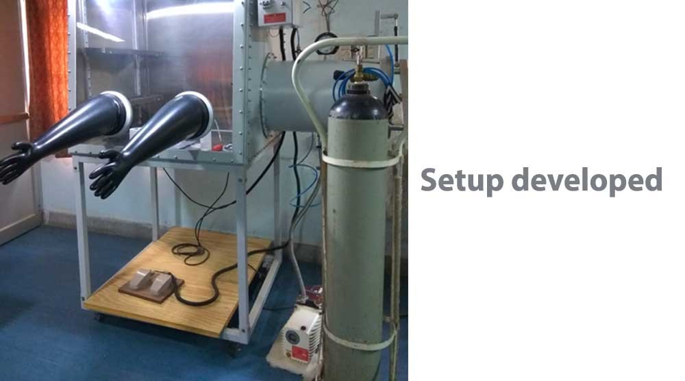
In this project a novel “Floating Film Technique” for formation of ordered thin film for large area organic electronic devices and demonstrated this for π- conjugated semiconducting polymer is proposed. The film preparation procedure of processible materials temporary cast on aliquid substrate followed by transfer on device substrateafter solidification over the liquid surface. Liquid substrateprovides the mobile substrate on which the nucleicanjoin with each other. π-π stacking betweenmulti-domains is also possible to fuse together for π- conjugated semiconducting polymer.
-
recent projects
-
 Design, Analysis and Fabrication of Prototype Magnetorheological fluid dampers for semi-active vibration control
Project Start:
Design, Analysis and Fabrication of Prototype Magnetorheological fluid dampers for semi-active vibration control
Project Start: -
 Development of waste heat recovery system with TEG and PCM for electrical applications
Project Start:
Development of waste heat recovery system with TEG and PCM for electrical applications
Project Start: -
Reforming of GHG: CO2 and CH4 over nanosize Ni-based catalyst to syngas
Project Start:
-
-
other projects